27.01.2015 -
From 28-30 January, A.P.E.
Research will be at Nano Tech
2015 (www.nanotechexpo.jp
), the world's biggest nanotechnology fair held each
year in Japan, this year being the
fourteenth edition.
The Trieste-based AREA Science
Park company, which specialises in
advanced nanotechnology
instruments and the development and
production of probe microscopes and ultra-high resolution motion
sensors, is a leading player in the "Nano
Japan Cluster Mission 2015" (
www.eu-japan.eu/nanotech-japan-cluster-mission-2015
). The mission, promoted by the EU-Japan Centre
for Industrial Cooperation (a
joint venture between the European Commission and the
Japanese government) is seeking to encourage collaborations between
companies in the field of nanomaterials, nanoscopic measurement and
analysis, and nanofabrication technologies. The programme involves
site visits, one-to-one meetings and seminars.
The trip to Japan will include an event organised by
ICE on 30
January, aimed at promoting innovative technologies from
Italy. The presentation will include some of the solutions
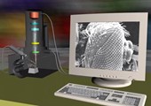
developed by A.P.E. (www.aperesearch.com
) such as the atomic force and tunnel effect
microscopes and the SNOM (scanning near field
optical microscope), which is used by universities and industrial
research centres to investigate materials and their surfaces, and
also in the fields of biology, chemistry and
medicine.
The Trieste spin-off has developed an international
reputation for technological excellence and already has a presence
in Asia, where it has forged an alliance with the Indian
Institute of Science (IISc), the largest institution of
its kind in India and one of the best-known in the world. The
laboratory at the IISc's Materials Research Centre (MRC) is
equipped with instruments supplied by A.P.E.
Research.
In addition to the main exhibition, Nano Tech 2015
will include a number of side events on topics such as water
management, energy saving, machines and
technologies used in conversion and for the treatment of
surfaces, materials and films, 3D decoration and printing, and
printable electronic components.